हमें कॉल करें now
07971189475
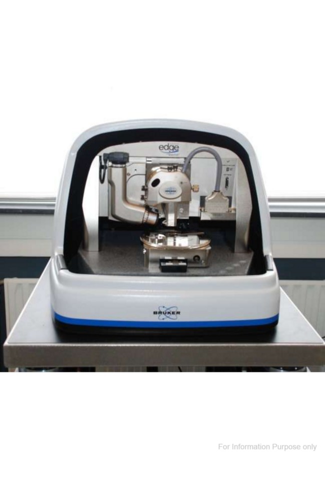

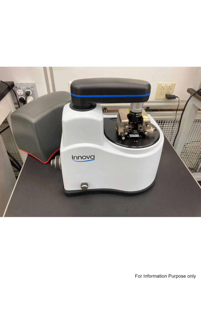
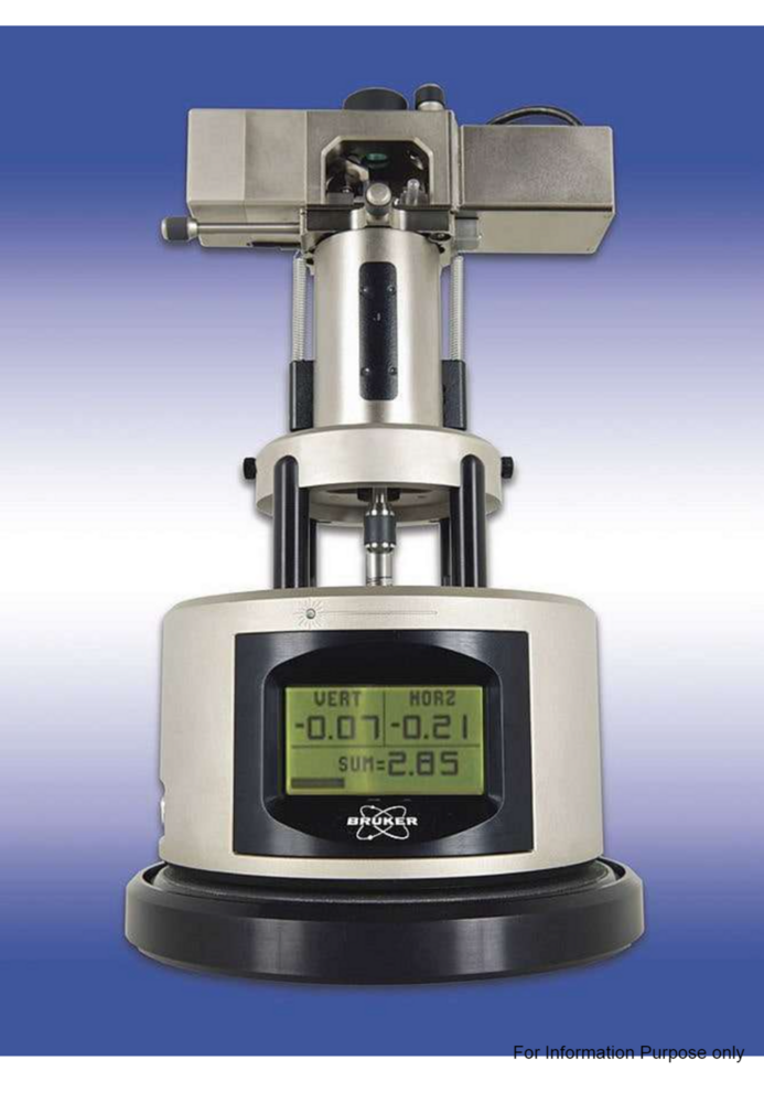
Specification
- स्पीड रेंज
- Up to 15 Hz scanning rate (line scan rate)
- कंट्रोल टाइप
- Motorized with computer control
- ग्लास टाइप
- Fused Silica Glass for sample stages and optical windows
- विशेषताएँ
- PeakForce Tapping technology, automated laser alignment, high-resolution imaging, low-noise electronics, closed-loop scan
- डिस्प्ले टाइप
- Integrated digital interface, external PC monitor
- तापमान प्रतिरोध
- Ambient to 60°C
- बिजली की आपूर्ति
- AC mains supplied, universal
- शेप
- Rectangular main frame
- सटीकता
- Z-axis noise <0.4 Å RMS (in air), XY-linearity <0.1%
- टाइप करें
- आयाम (एल* डब्ल्यू* एच)
- 585 mm x 576 mm x 322 mm
- उपकरण सामग्री
- Metal frame, vibration isolation materials, high-grade electronics
- पावर
- 100-240 V AC, 50/60 Hz
- वोल्टेज
- 100-240 V
- मटेरियल
- Precision-engineered metallic alloys, glass, composite polymer parts
- एप्लीकेशन
- High-resolution surface imaging, nano-scale characterization, materials science, life sciences, semiconductor analysis
- Max Scan Size
- 90 µm x 90 µm
- Data Output Formats
- TIFF, JPEG, proprietary formats, ASCII
- Vertical Range
- Up to 10 µm
- Noise Floor
- <0.4 Å RMS in air
- Connectivity
- USB, Ethernet
- Vibration Isolation
- Integrated active vibration control
- Sample Size
- Up to 210 mm diameter
- Weight
- Approximately 61 kg
- Scanner Type
- High-performance closed-loop XY and Z scanners
- Software
- NanoScope Analysis Suite
- Imaging Modes
- AFM, Tapping Mode, PeakForce Tapping, PhaseImaging, Nanoindentation
- Tip Positioning
- Automated and manual
Trade Information
- Minimum Order Quantity
- 1 टुकड़ा
- मुख्य निर्यात बाजार
- , , , , , , ,
Tell us about your requirement

Price: Â
Quantity
Select Unit
- 50
- 100
- 200
- 250
- 500
- 1000+
Additional detail
मोबाइल number
Email

अधिक Products in अस्पताल उपकरण Category
इनोर्बविक्ट हेल्थकेयर इंडिया प्राइवेट लिमिटेड लिमिटेड
GST : 27AADCI6120M1ZH
GST : 27AADCI6120M1ZH
|
दुकान नंबर 311, तीसरी मंजिल, जिओन मॉल, हिंजवडी,पुणे छावनी - 411027, महाराष्ट्र, भारत
फ़ोन :07971189475
Mr. Rajesh Meshram (Director)
Mob: 08068820202, + 91 9850558881
Mob: 08068820202, + 91 9850558881
- अस्पताल उपकरण
- Hospital Equipment
- नैदानिक उपकरण
- Medical Equipment
- Hospital Equipment
- न्यूरोलॉजी मशीन
- अल्ट्रासाउंड मशीन
- दंत चिकित्सा उपकरण
- Medical Equipment
- आईसीयू और एनआईसीयू उपकरण
- डायलिसिस उपकरण
- न्यूरोलॉजी उपकरण
- Medical Equipment
- रेडियोलॉजी उपकरण
- क्लिनिकल डायग्नोस्टिक्स
- सी-आर्म मशीन
- बंध्याकरण उपकरण
- एंटीवायरल ड्रग्स
 जांच भेजें
 एसएमएस भेजें
 मुझे निःशुल्क कॉल करें
INORBVICT HEALTHCARE INDIA PVT. LTD.
सर्वाधिकार सुरक्षित.(उपयोग की शर्तें)
इन्फोकॉम नेटवर्क प्राइवेट लिमिटेड . द्वारा विकसित एवं प्रबंधित
इन्फोकॉम नेटवर्क प्राइवेट लिमिटेड . द्वारा विकसित एवं प्रबंधित

